


“The nature of exponentials is that you push them and eventually disaster happens.” — Gordon Moore
In 1965, three years before he founded Intel, Gordon Moore predicted in an article he wrote for Electronics magazine that the number of transistors—the primary engine of computing power—on a semiconductor chip would double every year. Though at the time the count numbered only in the hundreds, he predicted that by 1975 it would reach 65,000. A decade later, after he had hit it on the nose, he revised his forecast, to a doubling of transistors every two years. Thus arose “Moore’s Law,” a phenomenon that has come to define the digital age.
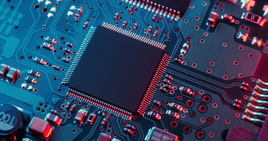
TSMC’s semiconductor contract manufacturing “fabs” in Hsinchu, Taiwan.
Moore based his predictions on economics. He looked at techniques for creating chains of transistors, or integrated circuits, and surmised that, the more transistors that could be crammed onto each quarter-square-inch piece of silicon, the less each individual transistor would cost, and the greater the demand would be for chips more chockablock with transistors. His was never a “law” in a physical sense, but a prophecy that became self-fulfilling when chipmakers and their customers adopted it as the basis for their long-term planning. When Moore first performed his estimations, there was plenty of room for engineering advances to shrink transistor size and grow the number. Over time, that became less and less the case. In fact, there is a less-celebrated derivation of Moore’s Law, known as Moore’s Second Law, which states that, even as the cost per transistor continues to drop, the cost to build a latest-generation chip fabrication plant doubles every four years. Then there is the unofficial corollary to that, what might be called Moore’s Third Law: with each new generation of chips, the exercise of designing and operating plants to fabricate them becomes exponentially more difficult, which winnows the number of chipmakers capable of keeping going the advancement of ever-more powerful chips to a very select group.
Over the past couple of years, the real-world implications of this “Third Law” have grown as advanced chip fabrication has collided with geopolitics. At this point, there are exactly two companies left on the planet capable of perpetuating the exponential shrinking of transistor size and concomitant growth in computing power foretold by Moore. One is South Korea-based Samsung Electronics.1 The other, accounting for the fabrication of 84% of the world’s most advanced chips, is TSMC, located just across the East China Sea in Taiwan, aka “The Most Dangerous Place on Earth,” in the words of a May 1, 2021 Economist cover story headline. The danger comes from the fraying of the strategic ambiguity that has governed relations between Taiwan, Mainland China, and the US for 70 years. In March 2021, Admiral Phil Davidson, who heads US naval operations in the Pacific, told Congress that he worries China could invade Taiwan as soon as 2027. He based his assessment on a variety of factors, from China’s long-running claim on what its leaders still view as a rogue territory, to the pace of China’s military buildup and erosion of US military superiority in the region, to the political clamp-down in Hong Kong, which has undercut the “carrot” approach of convincing Taiwan that a peaceful reunification could leave its people with a separate, democratic system of government. But chips also figure importantly into threats to the region’s security. As part of sanctions first enacted by the Trump administration, advanced chips like TSMC’s fabricated with even a small percentage of US-made equipment are banned from being sold to Huawei, the giant China-based 5G network equipment and smartphone manufacturer, and chipmakers have to specifically apply for US approval to ship to other Chinese companies. Any blow to Taiwan from a Chinese invasion that damages or otherwise stops production at TSMC facilities would be devastating to the global electronics industry and all those who depend on its products, i.e., nearly everyone. But, under the current sanctions regime, China is already effectively denied access to TSMC’s leading-edge chips anyway.
Any blow to Taiwan from a Chinese invasion that damages or otherwise stops production at TSMC facilities would be devastating to the global electronics industry and all those who depend on its products, i.e., nearly everyone. But, as it is, China is already effectively denied access to TSMC’s leading-edge chips anyway.
Such grim scenarios underly the urgency felt by EU and US leaders with regard to the security of their own chip supplies (an urgency only heightened by the recent global chip shortage caused by unexpected pandemic-related spikes in demand that caught all manner of chipmakers off guard, advanced and not). Leaders on both sides of the Atlantic have launched initiatives to encourage local companies to bring a portion of the world’s advanced fab capabilities back to native soil. But, as Igor Tishin, an Information Technology analyst at Harding Loevner, says, “Were it only that simple.” Tishin estimates that TSMC’s and Samsung’s technological lead over its rivals stretches from a minimum of 36 months to a decade or more. Even if onshoring efforts were successful (“and I think that’s a big IF,” Tishin says), he concurs with Jensen Huang, CEO of NVIDIA, a power user of TSMC and Samsung’s most advanced manufacturing services, who told The Wall Street Journal that large-scale chip production “won’t come for years.”
But if the West’s semiconductor supplies cannot be secured by using a local presence to restructure and decentralize the fabrication process, how can they be? To answer that, Tishin says, it helps to understand how Samsung and TSMC came to be the ultimate survivors of the Third Law.
From the Source
Their story begins in the early 1990s, when chip-making capabilities had advanced to the point that as many as 50 million individual transistors could be imprinted onto a single typical quarter-inch silicon square, or “die.” The size of each “node,” or distance an electrical current travelled from one end of a transistor (the “source”) to the other (the “drain”), had shrunk to just under 1 micron, or roughly 1/70 the width of a human hair.2 The frequency at which current was generated and turned off and on by the “gate,” the spigot controlling the flow of electricity between the source and drain, was around 100MHz, or about 100 million off/on cycles per second. All those cycles translated into a critical mass of processing power that gave rise to a major leap in the capabilities of personal computers and multimedia devices, leading, in turn, to exploding demand for high-end chips.
At the time, most major chipmakers, including Moore’s own Intel, operated on the integrated device manufacturer (IDM) model, designing and fabricating their own chips. To defray the enormous cost they incurred in building and maintaining fabrication facilities, these chipmakers would further monetize their investments by performing contract manufacturing for other companies (“fabless studios”) focused exclusively on chip design. But a few years earlier, a third business model emerged: the stand-alone foundry, dedicated to fabricating only other companies’ designs.
The first dedicated chip foundry was the Taiwan Semiconductor Manufacturing Corporation (later shortened to TSMC), created in 1987 when the government-owned Industrial Technology Research Institute split its chip design and fabrication functions. The stand-alone foundry model offered advantages of scale and specialization over the IDM approach, and, before long, fabless studios weren’t the only ones sending work to the new fabs. “Initially, it was just a way for the IDMs to manage their overflow, like a restaurant that outsources some of its pasta-making,” Tishin says. Eventually, though, as transistors shrank in size into the realm of nanometers (nm, or 1/1000 of a micron), the arrangement evolved into an ingrained part of the IDM business model for slowing the pace of investment. “When the leading-edge moved from 130 nm to 90 nm, the IDM might hold on to 60 percent of its fabrication production, focusing on 130 nm and above, and let an outsourcing fab handle the 90 nm node that otherwise would require a large incremental investment in more advanced tools and capacity.” From the perspective of the IDMs, after all, “it was still just pasta,” Tishin says, a capital-intensive but less core part of their business. But it also meant handing over to third parties an increasing amount of the know-how for making advanced circuitry.
Today, TSMC has 12 different fab facilities in operation or under construction, most located in and around its headquarters at the northern end of Taiwan. These include Fab No. 18 in the final stages of completion at a cost of US$20 billion, the third highest price tag for a building in history.
Today, TSMC has 12 different fab facilities in operation or under construction, most located in and around its headquarters in Hsinchu at the northern end of Taiwan. These include Fab No. 18 in the final stages of completion at a cost of US$20 billion, the third highest price tag for a building in history.3 At the center of the structure is a clean room the size of 22 soccer fields where the air will be scrubbed 2,000 times cleaner than a hospital operating room. (A single dust particle would wipe out tens of thousands of transistors.) Beneath the building, the legs of the entire frame of the clean room rest on ball bearings, to buttress against the island’s not infrequent earthquake activity, since the slightest quiver could send hundreds of millions of dollars’ worth of precision-imprinting implements skittering across silicon surfaces like a jostled turntable needle.
Advocates of public spending to support Western onshoring initiatives often cite the financial support the Taiwanese government has provided its local fab champions. In truth, Taiwan’s significant government investments in R&D tapered off years ago as the free cash flow generated by these businesses grew to comfortably accommodate their gargantuan capital funding needs. And capital is only part of TSMC’s competitive advantage. “You’re talking about a whole ecosystem built up over 30 years,” Tishin says. “You’re talking about generations of commitment to STEM education and deep relationships with every part of the supply chain. When you visit Hsinchu, you realize it’s not just TSMC’s production and R&D facilities—it’s everyone from equipment makers like ASML and AMAT to Apple and NVIDIA and all the other major players in the electronics chain that also have a major presence there.”
The complexity of chip manufacturing is difficult for many outside the industry to comprehend. While every fab starts with the same generic highly automated set of tools from the same handful of suppliers, the sensitivity of the equipment involved means that operating it depends heavily on the precise sequence of steps followed, materials used, and operator know-how. As an example, Tishin cites today’s most advanced fab processes, requiring the use of Netherlands-based ASML’s extreme ultraviolet (EUV) lithography machine, a US$180 million piece of equipment so advanced that ASML has produced only 100 so far (TSMC has half of them). The machine emits light waves about 15 times smaller than the previous leading-edge (deep ultraviolet or DUV) generation. These minute waves, generated by using lasers to turn droplets of liquified tin into plasma as hot as the sun, are aimed by mirrors at photosensitive material deposited on a round 12-inch silicon wafer. A kind of X-ray blanket known as a “mask” protects select parts of the deposited material and, in this way, patterns are developed, layer by layer, to form the transistors and transistor interconnects.

A visualization of what a Samsung or TSMC advanced integrated circuit looks like at about a billion times magnification.
Source: Semitracks Inc.
It takes about a dozen or so layers to get the transistors in place. Then the wafers are transferred to the older lithography machines, whose (relatively) cruder wavelengths are able to imprint the bulkier interconnects and power lines that comprise the higher floors of the stack.
A single layer can take over a day to finish, and with 90 layers in all, completing the process can consume 12 weeks total for each wafer. A state-of-the-art fab like the new No. 18 can turn out 100,000 completed wafers a month, each of which gets chopped into hundreds of square dies, the integrated circuit at the heart of each chip.
Importantly, these processes are all highly automated, executing already perfected techniques with minimal direct human involvement. Ramping up to produce the next-more-advanced and -tiny node requires creating production processes that are an order of magnitude more difficult to perfect. At times to help ensure success TSMC has run multiple R&D teams in parallel, competing with one another to see whose process variations win.
By 2017, the transistors stretched about as far across as a human fingernail grows every six seconds and were cycling 3 billion times a second. Within the span of a few months, Global Foundries and UMC announced that, for the first time, they would not pursue making more advanced chips. “They were, like, ‘We’re done,’” says Igor Tishin, an Information Technology analyst at Harding Loevner.
In 2017, a kind of physical boundary was finally reached. TSMC and Samsung each had begun delivery on their 10 nm dies. At this node, the transistors were roughly a few dozen atoms wide, about as far as a human fingernail grows every six seconds. Running at a frequency of 3 GHz, the spigot was cycling 3 billion times a second.
Within the span of a few months, Silicon Valley-based GlobalFoundries and TSMC’s Taiwan-based rival UMC announced that, for the first time, they would not pursue making more advanced dies. “They were, like, ‘We’re done,’” Tishin says. “To spend another US$15 billion-plus on new facilities, only to have TSMC and Samsung outrun them on both time-to-market and economics, was no longer a risk they were willing to take.”
Intel was the only other company that tried to keep pace. Rather than try to catch up with what would have been its equivalent of a 10 nm node,4 it jumped all the way from 14 nm to 7 nm, even as TSMC and Samsung hurtled ahead in early 2020 to 5 nm. “But Intel’s yield was just terrible,” Tishin says. “Every time they’d pull the dies out, way too many would have defects, killing their economics. They finally started shipping product anyway. They claim they’re doing better now, but I can’t imagine they’re making much money on their more advanced dies yet, because for every 100 they ship they could be throwing a good chunk away.”
Keeping the Flywheel Spinning
In 2018, Tishin had a conversation with a senior executive at one of TSMC’s largest customers, a US-based chip designer. He asked whether her company was worried about having so much of its supply dependent on a single supplier. “She said, ‘Of course, we are unhappy about it,’” Tishin recalls. The US company wasn’t afraid TSMC would exploit its near-monopoly status, since it was confident TSMC respected the delicate symbiosis of the chip supply ecosystem. What kept its management up at night were the risks—a typhoon, a geopolitical fracture—outside either company’s control. When they voiced these concerns to TSMC, “TSMC’s response was ‘OK, we get it. We can move more chip production closer to your own facilities. But it’s not going to be nearly as efficient for us so we may have to charge you 30% more for our services.’” Tishin said this US firm weighed the appreciable but remote and unquantifiable risk of catastrophic disruption against the far more definite and certain risk of putting itself in an uncompetitive cost position. It decided to keep the status quo. “She also said she was 100% sure their competitors looked at it the same way.”
Well before a smaller node reaches the market, anticipation is already influencing how many new features carmakers pack into future models and how many autonomous functions can be performed by robots. If, however, the rate of computational advancement slows, or becomes less certain, or more costly, that relationship can break down.
In this conversation we see the flywheel effect of Moore’s Law. Well before a smaller node reaches the market, anticipation is already influencing how many new features carmakers pack into future models and how many autonomous functions can be performed by robots, and further blurring the lines between physical reality and alternate realities generated by eyeglasses controlled with the flick of a wristband.5 If, however, the rate of computational advancement slows, or becomes less certain, or more costly, that relationship can break down; maybe the carmaker holds off on some features, or the social media giant shelves the Avatar-like glasses. That’s why Tishin’s US chip designer could barely entertain accepting a 30% jump in die prices, even if it meant kicking down the road the can of mitigating against a much greater disruption. Its whole business model—indeed, our entire economy—is based on the price of computing power leaping down, not up.
Source: World Semiconductor Trade Statistics, TS Lombard.
That doesn’t mean change isn’t coming. According to Tishin, even Samsung’s and TSMC’s pace of technological advance appears to have reached an inflection point. The reason is that transistors have grown so small that scientific fields like material science and atomic-level physics are rising in importance, as R&D teams pursue new types of exotic materials that can conduct electricity at this scale without frying the now-atomic-level conductors. The populations of South Korea and Taiwan have among the world’s highest densities of advanced degrees in electrical engineering, coding, and more traditional physics. But they have less homegrown expertise in the now-more-necessary fields. So, looking abroad actually makes sense, even if it means trading off some short-term economies of scale to establish more facilities in places like the US to help with recruiting and in-person collaboration and experimentation.
In early 2021, Samsung, which already has one fab in Austin, Texas, announced it is exploring sites in Texas, New York, and Arizona for a second US facility that could start to be operational by late 2023. TSMC has begun planning for its own fab in Arizona. Significantly, it has acquired enough property around the site to accommodate six such facilities, the combined capacity of which would rival the company’s largest “gigafabs” in Taiwan. While company officials have made clear that the “center of gravity” of their most advanced R&D and production will remain in Hsinchu, at that scale it’s conceivable the company could eventually supply a large portion of the needs of its US customers from US soil, while controlling costs to near where they are in Taiwan and keeping the flywheel spinning. The most realistic way to onshore US and European chip requirements, in other words, may be to let TSMC and Samsung do it instead of domestic also-rans.
In that event, Tishin says, he can imagine TSMC having the leverage to influence policy and do its part to turn back the semiconductor doomsday clock. “I could see them turning to Washington and saying: ‘Look, we’re going to build a gigafab here that will give you more physical security over your chip supply. Now we hope you can ease off on our business relations with China, which will also make China feel less backed into a corner.’” Deft maneuvering obviously will be required on other fronts as well, but Tishin sees the Biden administration’s recent reframing of the US’s economic policy toward China in terms of seizing “our Sputnik moment” as at least possibly a step toward chip de-escalation. “I think policymakers may eventually realize that the best way to help US companies preserve their technological edge against China is to work with the existing players to shore up the current supply chain framework and allow the specialization to follow its natural course, as opposed to trying to rewind the tape on 30 years of technological history.”
In the meantime, Samsung and TSMC have alerted customers to plan for delivery of 3 nm chips starting in late 2022. And TSMC recently announced it has moved past the R&D stage on 2 nm.
What did you think of this piece?
Contributors
Analyst Igor Tishin, PhD contributed research and viewpoints to this piece.
Endnotes
1As noted in our November 2020 Fundamental Thinking “The First Time in Memory,” Samsung is also part of an oligopoly that control’s the world’s supply of memory chips. While sharing some of the same manufacturing processes as logic chips (the “brains” that carry out computational tasks), memory chips merely store data and as such are essentially a commodity, much like wheat or airline seats.
2Over time, as discrepancies cropped up in how different manufacturers labelled and marketed their chips, the term “node” would come to lose its original meaning as a measurement of actual physical distance. Today, node is a proxy for feature scale signifying the generation of chips made with the same technology.
3The Great Mosque of Mecca, whose 16th-century footprint was expanded more than fivefold with Arab oil money in the latter half of the 20th century, is considered the most expensive building in modern times, costing US$100 billion in today’s money. No. 2 is the international thermonuclear experimental reactor in France, which some estimates put at a total cost of between US$45 billion and US$65 billion once it’s completed (currently targeted for 2025).
4In a further quirk of the chipmaking world, Intel has long used its own node scale for measuring the size of its transistors. What is widely considered a 10 nm node by fabs such as Samsung and TSMC is the equivalent of a 20 nm node at Intel. The company did recently announce that to minimize confusion and put its nomenclature on even footing with its rivals it plans to switch soon to the industry standard.
5“Facebook Is Building Wristband to Control Augmented Reality Glasses,” Bloomberg (March 18, 2021).
Disclosures
The “Fundamental Thinking” series presents the perspectives of Harding Loevner’s analysts on a range of investment topics, highlighting our fundamental research and providing insight into how we approach quality growth investing. For more detailed information regarding particular investment strategies, please visit our website, www.hardingloevner.com. Any statements made by employees of Harding Loevner are solely their own and do not necessarily express or relate to the views or opinions of Harding Loevner.
Any discussion of specific securities is not a recommendation to purchase or sell a particular security. Non-performance based criteria have been used to select the securities identified. It should not be assumed that investment in the securities identified has been or will be profitable. To request a complete list of holdings for the past year, please contact Harding Loevner.
There is no guarantee that any investment strategy will meet its objective. Past performance does not guarantee future results.
© 2024 Harding Loevner